Post by Wes Gear on Nov 26, 2013 22:02:53 GMT 10
Graphene: The quest for supercarbon
Graphene's dazzling properties promise a technological revolution, but Europe may have to spend a billion euros to overcome some fundamental problems.
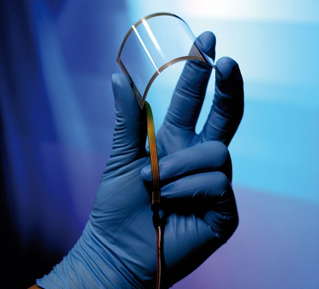
Graphene offers a way to make flexible and transparent smartphone screens.
Graphene is the thinnest substance ever made: a single sheet of carbon atoms arranged in a hexagonal honeycomb pattern. It is as stiff as diamond and hundreds of times stronger than steel — yet at the same time is extremely flexible, even stretchable. It conducts electricity faster at room temperature than any other known material, and it can convert light of any wavelength into a current. In the decade since graphene was first isolated, researchers have proposed dozens of potential applications, from faster computer chips and flexible touchscreens to hyper-efficient solar cells and desalination membranes.
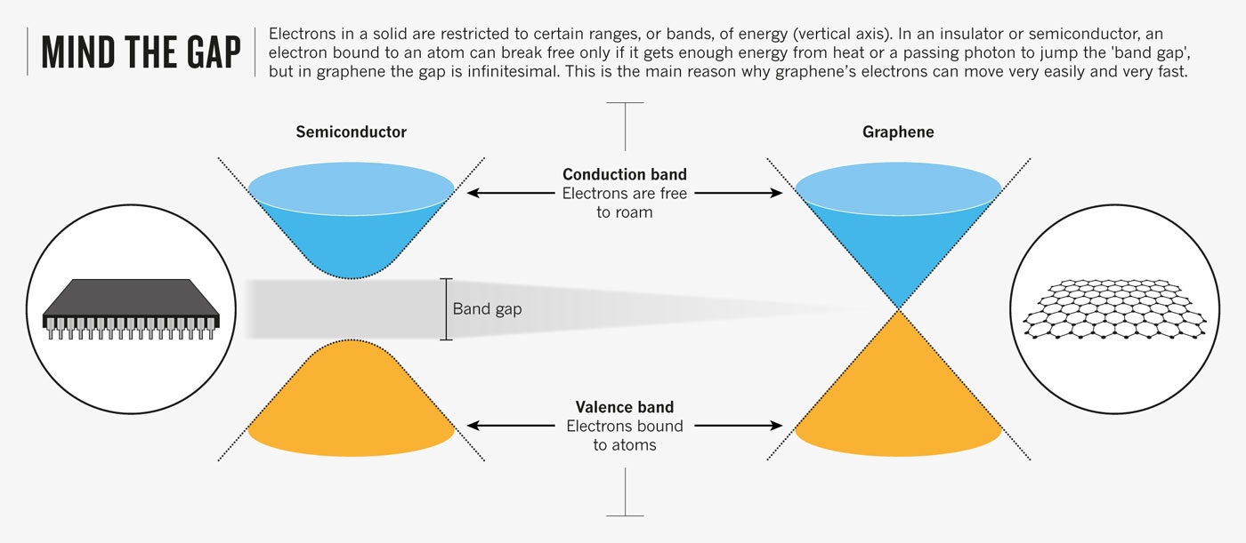
But harnessing graphene's qualities for practical use has proved a massive challenge. Graphene is complicated and expensive to make in large sheets, which usually have so many atomic-scale flaws and tears that they fail to match the amazing properties of the tiny flakes studied in the laboratory. And even if its quality were good, there are no well-established industrial methods for handling something so thin, or for integrating it with other materials to create useful products. What's more, graphene has a superweakness. Its electrons may be extremely mobile, but other properties make it fundamentally unsuitable for the sort of on–off switching that lies at the heart of digital electronics.
Hence Mr G's call to arms. The character was created in 2011 to help publicize a multinational push for a Graphene Flagship project: a decade-long, €1-billion (US$1.35-billion), all-European effort to take graphene from the laboratory bench to the factory floor. And not just graphene. The project's proponents also wanted to study more than a dozen other atomically thick materials discovered in graphene's wake — that, when sandwiched together with graphene, might help to overcome its limitations.
The campaign worked: the European Commission in Brussels gave its go-ahead to the graphene flagship project in January (see Nature 493, 585–586; 2013). Already the world's largest research effort on the material, encompassing hundreds of scientists across 17 European countries, it will grow even larger after the flagship puts out its first call for additional project proposals on 25 November.
The infusion of funds and energy has galvanized the graphene community, says Andrea Ferrari, director of the Cambridge Graphene Centre and chair of the flagship's executive board. Ferrari, whose office wall sports Mr G's poster, says “Nobody has been involved in anything this big before,”
Too many cooks?
But some question whether the programme is too big. Is an academia–industry collaboration, inevitably fettered by the bureaucracy of such a large venture, the best way to deliver a technological revolution? “This is not the way products are actually developed,” says Phaedon Avouris, a graphene and nanotechnology researcher at IBM's Thomas J. Watson Research Center in Yorktown Heights, New York. And some researchers involved in the project are concerned that political forces, rather than scientific priorities, will steer the dispersal of funds over the next few years.
Still, the flagship's prospects for success seem strong enough that national governments and industry partners, such as Nokia and Airbus, will collectively put up half its funding. (The European Commission will provide the rest.) “I hope that after ten years, technologies based on graphene or other layered materials are mainstream,” says the flagship's director Jari Kinaret, who is based at Chalmers University of Technology in Gothenburg, Sweden. Just as we now do with polymers, semiconductors and ceramics, he says, “we should take graphene for granted”.
The flagship programme is divided into 16 work packages, most of them targeted at developing applications such as high-frequency electronics, sensors and energy storage. Next week's call for proposals, worth €9 million, comes at the beginning of a €54-million ramp-up phase that is expected to deliver the first wave of prototypes by 2016.
But there will be no graphene computer chips, graphene sensors or graphene solar cells without a steady supply of graphene itself. One of the flagship's first and biggest challenges is to find more economical and reliable ways to produce high-quality sheets of the material.
Most research laboratories still make graphene using the method pioneered in 2004 by Andre Geim and Konstantin Novoselov at the University of Manchester, UK, who went on to win the 2010 Nobel Prize in Physics for their studies. Geim and Novoselov found that they just had to touch a strip of household sticky tape to ordinary graphite — which consists of billions of layers of graphene stacked on top of one another — and they could peel off thin flakes of carbon. By repeatedly splitting those flakes, they were eventually left with graphene2. This was a technique that any laboratory could use, and graphene research exploded.
But the method is much too slow and finicky for industrial-scale production. Just one micrometre-sized flake made in this way can cost more than $1,000 — making it, gram for gram, one of the most expensive materials on Earth.
The leading alternative3 relies on chemical vapour deposition (CVD), whereby methane is piped over a catalytic copper foil heated to about 1,000 °C. As the methane breaks down, small islands of pure carbon begin to grow on the foil, linking together to form a patchwork polycrystalline sheet of graphene. Harsh chemicals are then used to etch away the copper to free a sheet of graphene tens of centimetres wide, which can be transferred to a silica or polymer substrate. That process brings costs below $100,000 per square metre, but the product is often riddled with defects, impairing its electrical properties and making it much weaker than flakes produced by the sticky-tape method.
Read More:
Graphene's dazzling properties promise a technological revolution, but Europe may have to spend a billion euros to overcome some fundamental problems.
Graphene offers a way to make flexible and transparent smartphone screens.
Graphene is the thinnest substance ever made: a single sheet of carbon atoms arranged in a hexagonal honeycomb pattern. It is as stiff as diamond and hundreds of times stronger than steel — yet at the same time is extremely flexible, even stretchable. It conducts electricity faster at room temperature than any other known material, and it can convert light of any wavelength into a current. In the decade since graphene was first isolated, researchers have proposed dozens of potential applications, from faster computer chips and flexible touchscreens to hyper-efficient solar cells and desalination membranes.
But harnessing graphene's qualities for practical use has proved a massive challenge. Graphene is complicated and expensive to make in large sheets, which usually have so many atomic-scale flaws and tears that they fail to match the amazing properties of the tiny flakes studied in the laboratory. And even if its quality were good, there are no well-established industrial methods for handling something so thin, or for integrating it with other materials to create useful products. What's more, graphene has a superweakness. Its electrons may be extremely mobile, but other properties make it fundamentally unsuitable for the sort of on–off switching that lies at the heart of digital electronics.
Hence Mr G's call to arms. The character was created in 2011 to help publicize a multinational push for a Graphene Flagship project: a decade-long, €1-billion (US$1.35-billion), all-European effort to take graphene from the laboratory bench to the factory floor. And not just graphene. The project's proponents also wanted to study more than a dozen other atomically thick materials discovered in graphene's wake — that, when sandwiched together with graphene, might help to overcome its limitations.
The campaign worked: the European Commission in Brussels gave its go-ahead to the graphene flagship project in January (see Nature 493, 585–586; 2013). Already the world's largest research effort on the material, encompassing hundreds of scientists across 17 European countries, it will grow even larger after the flagship puts out its first call for additional project proposals on 25 November.
The infusion of funds and energy has galvanized the graphene community, says Andrea Ferrari, director of the Cambridge Graphene Centre and chair of the flagship's executive board. Ferrari, whose office wall sports Mr G's poster, says “Nobody has been involved in anything this big before,”
Too many cooks?
But some question whether the programme is too big. Is an academia–industry collaboration, inevitably fettered by the bureaucracy of such a large venture, the best way to deliver a technological revolution? “This is not the way products are actually developed,” says Phaedon Avouris, a graphene and nanotechnology researcher at IBM's Thomas J. Watson Research Center in Yorktown Heights, New York. And some researchers involved in the project are concerned that political forces, rather than scientific priorities, will steer the dispersal of funds over the next few years.
Still, the flagship's prospects for success seem strong enough that national governments and industry partners, such as Nokia and Airbus, will collectively put up half its funding. (The European Commission will provide the rest.) “I hope that after ten years, technologies based on graphene or other layered materials are mainstream,” says the flagship's director Jari Kinaret, who is based at Chalmers University of Technology in Gothenburg, Sweden. Just as we now do with polymers, semiconductors and ceramics, he says, “we should take graphene for granted”.
The flagship programme is divided into 16 work packages, most of them targeted at developing applications such as high-frequency electronics, sensors and energy storage. Next week's call for proposals, worth €9 million, comes at the beginning of a €54-million ramp-up phase that is expected to deliver the first wave of prototypes by 2016.
But there will be no graphene computer chips, graphene sensors or graphene solar cells without a steady supply of graphene itself. One of the flagship's first and biggest challenges is to find more economical and reliable ways to produce high-quality sheets of the material.
Most research laboratories still make graphene using the method pioneered in 2004 by Andre Geim and Konstantin Novoselov at the University of Manchester, UK, who went on to win the 2010 Nobel Prize in Physics for their studies. Geim and Novoselov found that they just had to touch a strip of household sticky tape to ordinary graphite — which consists of billions of layers of graphene stacked on top of one another — and they could peel off thin flakes of carbon. By repeatedly splitting those flakes, they were eventually left with graphene2. This was a technique that any laboratory could use, and graphene research exploded.
But the method is much too slow and finicky for industrial-scale production. Just one micrometre-sized flake made in this way can cost more than $1,000 — making it, gram for gram, one of the most expensive materials on Earth.
The leading alternative3 relies on chemical vapour deposition (CVD), whereby methane is piped over a catalytic copper foil heated to about 1,000 °C. As the methane breaks down, small islands of pure carbon begin to grow on the foil, linking together to form a patchwork polycrystalline sheet of graphene. Harsh chemicals are then used to etch away the copper to free a sheet of graphene tens of centimetres wide, which can be transferred to a silica or polymer substrate. That process brings costs below $100,000 per square metre, but the product is often riddled with defects, impairing its electrical properties and making it much weaker than flakes produced by the sticky-tape method.
Read More: